1
Date: 08/10/05 SP6213, SP6214 Micropower, SC-70, 100mA CMOS LDO Regulator © Copyright 2005 Sipex Corporation
Tiny 5-pin SC-70 Package
Guaranteed 100 mA Output
2.5% Output Voltage Accuracy
Low Dropout Voltage: 250 mV at 100mA
Low Quiescent Current: 65 ĶA
Low Ground Current: 135 ĶA @ I
L
= 100mA
Low Shutdown Current: 1ĶA MAX
Current Limit: 190mA
Thermal Shutdown: 168įC
Good Load and Line Regulation
Fast Transient Response: T
ON
/T
OFF
=80Ķs
Low Temperature Coefficient
Unconditionally Stable with 1ĶF Ceramic
Fixed Outputs: 1.8V, 2.5V, 2.7V, 2.85V, 3.0V, 3.3V, 5V
100mA Replacement for 80mA MIC5213 & TC1016
(SP6213)
100mA Replacement for 80mA NCP512 (SP6214)
Micropower, SC-70, 100mA CMOS LDO Regulator
SP6213/SP6214
DESCRIPTION
The SP6213/4 is a 100mA CMOS linear voltage regulator offered in an SC-70 package that reduces board space
requirements by 50% over a SOT-23 package. The SP6213/4 features low dropout voltage (250mV at 100mA ), low
ground current (135ĶA at full load) and low, 65ĶA quiescent current. Designed specifically for hand-held, battery
powered devices, the device includes an enable/shutdown pin. Regulator ground current increases only slightly in
dropout to extend battery life. The SP6213/4 is offered in an industry standard 5-pin SC-70 package. SP6213/4 is
available in 1.8V, 2.5V, 2.7V, 2.85V, 3.0V, 3.3V and 5.0V fixed output voltages.
FEATURES
ģ
Digital Cordless Phones
Cellular Phones
PDAs
Digital Still Cameras
MP3 Players
Battery-Powered Equipment
Medical Devices
Data Cable
APPLICATIONS
*connect to GND for enhanced
thermal performance
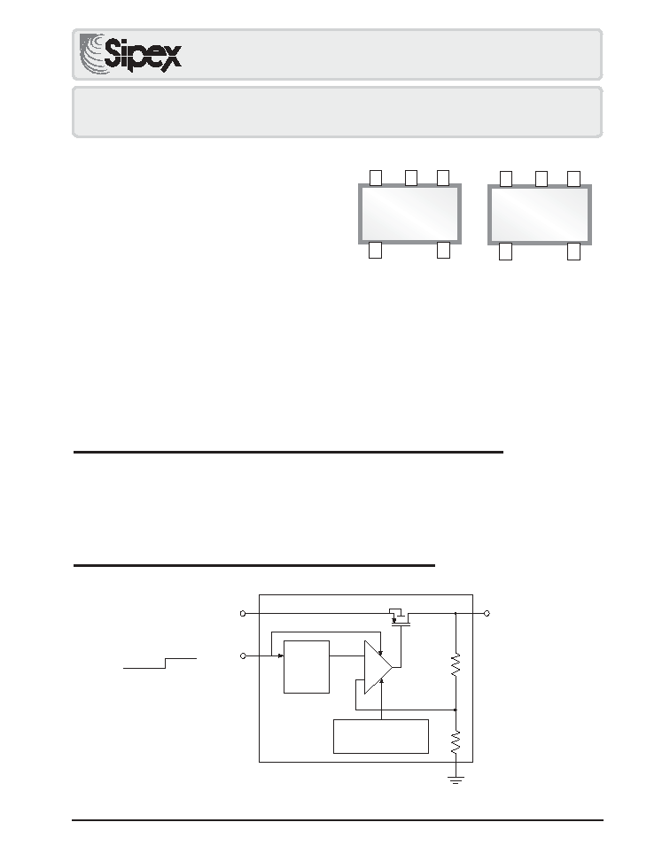
SP6213
5 Pin SC70
5
V
IN
1
EN
3
GND
4
V
OUT
2
NC*
FUNCTIONAL DIAGRAM
V
OUT
+
≠
Current Limit
& Thermal Shutdown
1.25V
Bandgap
Reference
V
IN
GND
EN
Enable
Shutdown
SP6214
5 Pin SC70
5
V
IN
1
EN
3
GND
4
V
OUT
2
NC*
Now Available in Lead Free Packaging
2
Date: 08/10/05 SP6213, SP6214 Micropower, SC-70, 100mA CMOS LDO Regulator © Copyright 2005 Sipex Corporation
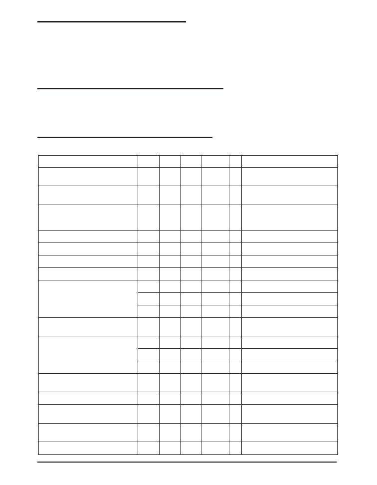
Supply Input Voltage (V
IN
)...................................-2V to 7V
Output Voltage (V
OUT
)...............................-0.6 to (V
IN
+1V)
Enable Input Voltage (V
EN
).............................-2V to 7V
Power Dissipation (P
D
)............Internally Limited, Note 3
Lead Temperature (soldering 5s)..........................260įC
Storage Temperature............................-65įC to +150įC
Input Voltage (V
IN
) ................................... +2.5V to +6V
Enable Input Voltage (V
EN
) ...................... ZeroV to +6V
Junction Temperature (T
J
) ................. -40įC to +125įC
R
E
T
E
M
A
R
A
P
N
I
M
P
Y
T
X
A
M
S
T
I
N
U
S
N
O
I
T
I
D
N
O
C
V
(
,
y
c
a
r
u
c
c
A
e
g
a
t
l
o
V
t
u
p
t
u
O
T
U
O
)
5
.
2
-
4
-
5
.
2
4
%
V
d
e
i
f
i
c
e
p
s
m
o
r
f
n
o
i
t
a
i
r
a
V
T
U
O
e
r
u
t
a
r
e
p
m
e
T
e
g
a
t
l
o
V
t
u
p
t
u
O
,
4
e
t
o
N
,
t
n
e
i
c
i
f
f
e
o
C
(V
T
U
O
/ )
T
0
6
/
m
p
p
į C
e
g
a
t
l
o
V
y
l
p
p
u
S
m
u
m
i
n
i
M
0
5
.
2
5
5
.
2
5
7
.
2
0
7
.
2
5
8
.
2
0
0
.
3
V
I
T
U
O
A
Ķ
0
0
1
=
I
T
U
O
A
m
0
5
=
I
T
U
O
A
m
0
0
1
=
(
,
n
o
i
t
a
l
u
g
e
R
e
n
i
L
V
T
U
O
V
/
N
I
)
5
0
.
0
2
.
0
V
/
%
V
N
I
V
(
=
T
U
O
V
6
o
t
)
V
5
.
0
+
n
o
i
t
a
l
u
g
e
R
e
n
i
L
V
8
.
1
-
3
1
2
6
P
S
5
0
.
0
2
.
0
V
/
%
V
N
I
V
6
o
t
V
8
.
2
=
(
,
5
e
t
o
N
,
n
o
i
t
a
l
u
g
e
R
d
a
o
L
V
T
U
O
)
4
.
0
8
.
0
%
I
L
V
,
A
m
0
0
1
o
t
A
m
1
.
0
=
N
I
V
=
T
U
O
V
1
+
n
o
i
t
a
l
u
g
e
R
d
a
o
L
V
8
.
1
-
3
1
2
6
P
S
4
.
0
8
.
0
%
I
L
V
,
A
m
0
0
1
o
t
A
m
1
.
0
=
N
I
V
0
.
3
=
V
(
,
6
e
t
o
N
,
e
g
a
t
l
o
V
t
u
o
p
o
r
D
N
I
V
≠
T
U
O
)
5
2
.
0
4
V
m
I
L
0
0
1
=
ĶA
0
3
1
0
5
2
V
m
I
L
A
m
0
5
=
0
5
2
0
0
5
V
m
I
L
A
m
0
0
1
=
I
(
,
t
n
e
r
r
u
C
t
n
e
c
s
e
i
u
Q
D
N
G
)
1
0
.
0
5
6
1
5
2
1
ĶA
V
N
E
)
n
w
o
d
t
u
h
S
(
V
4
.
0
V
N
E
I
,
)
g
n
i
t
a
r
e
p
O
(
V
6
.
1
L
A
Ķ
0
=
I
(
,
7
e
t
o
N
,
t
n
e
r
r
u
C
n
i
P
d
n
u
o
r
G
D
N
G
)
5
6
5
2
1
ĶA
V
N
E
I
,
V
6
.
1
L
0
0
1
=
ĶA
0
0
1
5
7
1
ĶA
V
N
E
I
,
V
6
.
1
L
A
m
0
5
=
5
3
1
0
5
2
ĶA
V
N
E
I
,
V
6
.
1
L
A
m
0
0
1
=
,
o
i
t
a
R
n
o
i
t
c
e
j
e
R
y
l
p
p
u
S
r
e
w
o
P
)
R
R
S
P
(
4
7
0
4
B
d
I
,
z
H
0
0
1
=
y
c
n
e
u
q
e
r
F
L
A
m
0
1
=
I
,
z
H
k
0
0
4
=
y
c
n
e
u
q
e
r
F
L
A
m
0
1
=
I
(
,
t
i
m
i
L
t
n
e
r
r
u
C
L
C
)
0
2
1
0
9
1
0
5
3
A
m
t
i
m
i
L
l
a
m
r
e
h
T
8
6
1
3
5
1
į C
n
O
s
n
r
u
T
f
f
O
s
n
r
u
T
(
,
n
o
i
t
a
l
u
g
e
R
l
a
m
r
e
h
T
V
T
U
O
/P
D
,
)
8
e
t
o
N
5
0
.
0
W
/
%
e
(
e
s
i
o
N
t
u
p
t
u
O
O
N
)
0
5
2
s
m
r
V
Ķ
I
L
C
,
A
m
0
5
=
L
z
H
k
0
0
1
o
t
z
H
0
1
,
F
Ķ
1
=
(Note 1) These are stress ratings only and functional
operation of the device at these ratings or any other
above those indicated in the operation sections of the
specifications below is not implied. Exposure to absolute
maximum rating conditions for extended periods of time
may affect reliability.
ABSOLUTE MAXIMUM RATINGS (Note 1)
OPERATING RATINGS (Note 2)
Thermal Resistance ................................... (Note 3)
SC-70-5 (
JA
) .............................. 330įC/W
ELECTRICAL CHARACTERISTICS
V
IN
= V
OUT
+0.5V, I
L
= 100ĶA, C
IN
= 1ĶF, C
OUT
= 1ĶF, T
J
= 25
į
C , unless otherwise noted. The denotes the specifications which apply over the full
operating temperature range, unless otherwise specified.

3
Date: 08/10/05 SP6213, SP6214 Micropower, SC-70, 100mA CMOS LDO Regulator © Copyright 2005 Sipex Corporation
Note 1. Exceeding the absolute maximum rating may damage the device.
Note 2. The device is not guaranteed to function outside its operating rating.
Note 3. The maximum allowable power dissipation at any T
A
(ambient temperature) is P
D (MAX)
= (T
J
(MAX)
≠ T
A
) /
JA
.
Exceeding the maximum allowable power dissipation will result in excessive die temperature, and the
regulator will go into thermal shutdown. The
JA
of the SP6213/4 (SC-70-5) is 330įC/W mounted on a PC
board with minimum copper area (see "Thermal Considerations" section for further details).
Note 4. Output voltage temperature coefficient is defined as the worst case voltage change divided by the total
temperature range.
Note 5. Load Regulation is measured at constant junction temperature using low duty cycle pulse testing. Parts
are tested for load regulation in the load range. Changes in output voltage due to heating effects are
covered by the thermal regulation specification.
Note 6. Dropout Voltage is defined as the input to output differential at which the output voltage drops 2% below
its nominal value measured at 0.5V differential. Not applicable to output voltages less than 2.7V.
Note 7. Ground pin current is the regulator quiescent current. The total current drawn from the supply is the sum
of the load current plus the ground pin current.
Note 8. Thermal regulation is defined as the change in output voltage at a time "t" after a change in power
dissipation is applied, excluding load or line regulation effects. Specifications are for a 100mA load pulse
at V
IN
= 6V for t = 10ms.
Note 9. Devices are ESD sensitive. Handling precautions are recommended.
R
E
T
E
M
A
R
A
P
N
I
M
P
Y
T
X
A
M
S
T
I
N
U
S
N
O
I
T
I
D
N
O
C
T
U
P
N
I
E
L
B
A
N
E
V
(
,
e
g
a
t
l
o
V
w
o
L
-
c
i
g
o
L
t
u
p
n
I
e
l
b
a
n
E
L
I
)
4
.
0
V
n
w
o
d
t
u
h
S
r
o
t
a
l
u
g
e
R
V
(
,
e
g
a
t
l
o
V
h
g
i
H
-
c
i
g
o
L
t
u
p
n
I
e
l
b
a
n
E
H
I
)
6
.
1
V
d
e
l
b
a
n
E
r
o
t
a
l
u
g
e
R
I
(
,
t
n
e
r
r
u
C
t
u
p
n
I
e
l
b
a
n
E
L
I
I
(
,
)
H
I
)
1
0
.
0
1
ĶA
V
L
I
<
V
4
.
0
1
0
.
0
1
ĶA
V
H
I
>
V
6
.
1
T
(
e
m
i
T
n
o
n
r
u
T
N
O
)
0
8
5
6
1
Ķs
I
T
U
O
A
m
0
5
=
T
(
e
m
i
T
f
f
o
n
r
u
T
N
F
O
)
0
8
0
3
5
7
1
5
3
Ķs
I
T
U
O
A
Ķ
0
0
1
=
I
T
U
O
A
m
0
0
1
=
ELECTRICAL CHARACTERISTICS
V
IN
= V
OUT
+0.5V, I
L
= 100ĶA, C
IN
= 1ĶF, C
OUT
= 1ĶF, T
J
= 25
į
C , unless otherwise noted. The denotes the specifications which apply over
the full operating temperature range, unless otherwise specified.
PIN NUMBER
PIN NAME
SP6214 DESCRIPTION (FUNCTION)
1
V
IN
Supply Input
2
GND
Ground Connection
3
EN
Enable / Shutdown (Logic high=enable; logic low = shutdown)
4
NC
No Connection
5
V
OUT
Regulator Output
PIN DESCRIPTION
PIN NUMBER
PIN NAME
SP6213 DESCRIPTION (FUNCTION)
1
EN
Enable / Shutdown (Logic high=enable; logic low = shutdown)
2
NC
No Connection
3
GND
Ground Connection
4
V
OUT
Regulator Output
5
V
IN
Supply Input

4
Date: 08/10/05 SP6213, SP6214 Micropower, SC-70, 100mA CMOS LDO Regulator © Copyright 2005 Sipex Corporation
General Overview
Enable/Shutdown Operation
The SP6213/4 is turned off by pulling the EN
pin low and turned on by pulling it high. If this
enable/shutdown feature is not required, EN
should be tied to V
IN
to keep the regulator
output on at all times.
Input Capacitor
Any good quality ceramic or tantalum capaci-
tor may be used at the input. A small capacitor
of about 1ĶF is required from V
IN
to GND if, for
instance, a battery is used as the input.
Output Capacitor
An output capacitor is required between V
OUT
and GND to prevent oscillation. The minimum
size of the output capacitor is a 0.47 ĶF
ceramic. The given datasheet values relate to
an IC with a ceramic output capacitor of 1ĶF.
Larger values make the IC more stable which
means an improvement of the regulator's
transient response. For a lower output cur-
rent, the output capacitance can be chosen
smaller in order to have the same output
stability.
No Load Stability
The SP6213/4 will remain stable and in regu-
lation with no external load (other than the
internal voltage driver) unlike many other volt-
age regulators. This is especially important in
CMOS RAM keep-alive applications.
Thermal Considerations
The SP6213/4 is designed to provide 100 mA
of continuous current in a very tiny package.
Maximum power dissipation can be calcu-
lated based on the output current and the
voltage drop across the part. To determine
the maximum power dissipation of the pack-
age, use the junction-to-ambient thermal re-
sistance of the device and the following basic
equation:
P
D
= (T
J(max)
- T
A
) /
JA
T
J(max)
is the maximum junction temperature
of the die and is 125įC. T
A
is the ambient
operating temperature.
JA
is the junction-to-
ambient thermal resistance for the regulator
and is layout dependent. The actual power
dissipation of the regulator circuit can be
determined using one simple equation:
P
D
= (V
IN
- V
OUT
)*I
OUT
+ V
IN
*I
GND
Substituting P
D(max)
for P
D
and solving for the
operating conditions that are critical to the
application will give the maximum operating
conditions for the regulator circuit. For ex-
ample, if we are operating the SP6213/4 at
3.0V output at room temperature, with a mini-
mum footprint layout, we can determine the
maximum input voltage for a set output cur-
rent:
P
D(max)
= [(125įC -25įC) / (330įC/W)]
= 303 mW.
To prevent the device from entering thermal
shutdown, maximum power dissipation can
not be exceeded. Using the output voltage of
3.0V and an output current of 100 mA, the
maximum input voltage can be determined.
Ground pin current can be taken from the
electrical specifications table (0.135 mA at
100 mA). The maximum input voltage is de-
termined as follows:
303mW = (V
IN
≠ 3.0V)*100mA + V
IN
*0.135mA
After calculations, we find that the maximum
input voltage of a 3.0V application at 100mA
of output current in an SC-70-5 package is
6.02V.
THEORY OF OPERATION

5
Date: 08/10/05 SP6213, SP6214 Micropower, SC-70, 100mA CMOS LDO Regulator © Copyright 2005 Sipex Corporation
27įC, V
IN
=4V, I
L
= 0.1mA, C
IN
= C
OUT
= 1ĶF unless otherwise specified.
3
3.01
3.02
3.03
3.04
3.05
-50
0
50
100
150
Temperature (įC)
V
OUT
(V)
V
IN
=4V
V
IN
=5.5V
V
IN
=7V
2.99
3
3.01
3.02
3.03
3.04
3.05
-50
0
50
100
150
Temperature (įC)
V
OUT
(V)
V
IN
=4V
V
IN
=5.5V
V
IN
=7V
2.97
2.98
2.99
3
3.01
3.02
3.03
3.04
-50
0
50
100
150
Temperature (įC)
V
OUT
(V)
V
IN
=4
V
V
IN
=5.5V
V
IN
=7V
2.95
2.96
2.97
2.98
2.99
3
3.01
3.02
3.03
3.04
-50
0
50
100
150
Temperature (įC)
V
OUT
(V)
V
IN
=4V
V
IN
=5.5V
V
IN
=7V
0
50
100
150
200
-50
0
50
100
150
Temperature (įC)
Iq (uA)
V
IN
=4V
V
IN
=5.5V
V
IN
=7V
0
0.05
0.1
0.15
0.2
0.25
-40
-20
0
20
40
60
80
100
120
140
Temperature (įC)
V
DROPOUT
(V)
I
LOAD
=10mA
I
LOAD
=50mA
I
LOAD
=100mA
Line Regulation at 27įC
3.015
3.025
3.035
3.045
3
4
5
6
7
V
IN
(V)
V
OUT
(V)
Io=0.1mA
Io=10mA
Io=50mA
Io=100mA
3.025
3.030
3.035
3.040
3.045
0
20
40
60
80
100
Io (mA)
V
OUT
(V)
Vin = 4V
Vin = 5.5V
Vin = 7V
3.025
3.030
3.035
3.040
3.045
0
20
40
60
80
100
V
IN
= 4V
V
IN
= 5.5V
V
IN
= 7V
Output Voltage vs. Temperature (I
OUT
= 0.1mA)
Output Voltage vs. Temperature (I
OUT
= 10mA)
Output Voltage vs. Temperature (I
OUT
= 50mA)
Output Voltage vs. Temperature (I
OUT
= 100mA)
Quiescent Current vs. Temperature (I
OUT
= 0A)
Dropout Voltage vs. Temperature
Output Voltage vs. Output Current
Output Voltage vs. Input Voltage
TYPICAL PERFORMANCE CHARACTERISTICS

6
Date: 08/10/05 SP6213, SP6214 Micropower, SC-70, 100mA CMOS LDO Regulator © Copyright 2005 Sipex Corporation
27įC, V
IN
=4V, I
L
= 0.1mA, C
IN
= C
OUT
= 1ĶF unless otherwise specified.
0
50
100
150
200
250
0
25
50
75
100
Io (mA)
V
DROPOUT
(mV)
0
20
40
60
80
100
0
1
2
3
4
5
6
7
V
IN
(V)
0
1
2
3
4
5
6
EN = Vin
EN = 0V
Iq (uA)
0
50
100
150
200
0
25
50
75
100
Io (mA)
I
GND
(uA)
V
IN
= 4V
V
IN
= 5.5V
V
IN
= 7V
0
25
50
75
100
125
150
175
3
4
5
6
7
V
IN
(V)
I
GND
(uA)
Io=0.1mA
Io=10mA
Io=50mA
Io=100mA
Quiescent Current vs. Input Voltage
Ground Current vs. Output Current
Ground Current vs. Input Voltage
Dropout Voltage vs. Output Current
SP6213-3.0V
OUT
fixed
V
EN
is toggled, V
IN
=4V
CTE
I
OUT
=100uA
C
IN
=C
OUT
=1uF Cer. Cap
V
OUT
V
EN
3V
2V
1V
0V
4V
2V
0V
Turn-on Characteristic (V
IN
= 4V, I
OUT
= 100
ĶA)
Turn-on Characteristic (V
IN
= 4V, I
OUT
=100mA)
SP6213-3.0V
OUT
fixed
V
EN
is toggled, V
IN
=7V
CTE
I
OUT
=100uA
C
IN
=C
OUT
=1uF Cer. Cap
V
OUT
V
EN
3V
2V
1V
0V
4V
2V
0V
Turn-on Characteristic (V
IN
= 7V, I
OUT
= 100
ĶA)
SP6213-3.0V
OUT
fixed
V
EN
is toggled, V
IN
=7V
CTE
I
OUT
=100mA
C
IN
=C
OUT
=1uF Cer. Cap
V
OUT
V
EN
3V
2V
1V
0V
4V
2V
0V
Turn on Time (V
IN
= 7V, I
OUT
= 100mA)
TYPICAL PERFORMANCE CHARACTERISTICS
7
Date: 08/10/05 SP6213, SP6214 Micropower, SC-70, 100mA CMOS LDO Regulator © Copyright 2005 Sipex Corporation
SP6213-3.0V
OUT
fixed
V
EN
is toggled, V
IN
=4V
CTE
I
OUT
=100uA
C
IN
=C
OUT
=1uF Cer. Cap
V
OUT
V
EN
200mA
0mA
3V
2V
0V
4V
2V
0V
200mA
I
IN
(V
IN
= 4V, I
OUT
= 100
ĶA)
SP6213-3.0V
OUT
fixed
V
EN
is toggled, V
IN
=4V
CTE
I
OUT
=100uA
C
IN
=C
OUT
=1uF Cer. Cap
V
OUT
V
EN
3V
2V
1V
0V
4V
2V
0V
Turn off Time (V
IN
=4V, I
OUT
=100
ĶA)
Turn off time
SP6213-3.0V
OUT
fixed
V
EN
is toggled, V
IN
=4V
CTE
I
OUT
=100mA
C
IN
=C
OUT
=1uF Cer. Cap
V
OUT
V
EN
3V
2V
1V
0V
4V
2V
0V
Turn off Time (V
IN
= 4V, I
OUT
= 100mA)
SP6213-3.0V
OUT
fixed
V
EN
is toggled, V
IN
=7V
CTE
I
OUT
=100uA
C
IN
=C
OUT
=1uF Cer. Cap
V
OUT
V
EN
3V
2V
1V
0V
4V
2V
0V
Turn off Time (V
IN
= 7V, I
OUT
= 100
ĶA)
SP6213-3.0V
OUT
fixed
V
EN
is toggled, V
IN
=7V
CTE
I
OUT
=100mA
C
IN
=C
OUT
=1uF Cer. Cap
V
OUT
V
EN
3V
2V
1V
0V
4V
2V
0V
Turn off Time (V
IN
= 7V, I
OUT
= 100mA)
SP6213-3.0V
OUT
fixed
V
EN
is toggled, V
IN
=4V
CTE
I
OUT
=100mA
C
IN
=C
OUT
=1uF Cer. Cap
V
OUT
V
EN
200mA
0mA
3V
2V
0V
4V
2V
0V
200mA
I
IN
In-Rush Current (V
IN
= 4V, I
OUT
= 100mA)
SP6213-3.0V
OUT
fixed
V
IN
=4V
CTE
C
IN
=C
OUT
=1uF Cer. Cap
T
R
=T
F
=100ns
I
OUT
100uA
V
OUT
20mV
10mV
0mV
-10mV
100mA
0mA
Load Transient Response (V
IN
= 4V)
SP6213-3.0V
OUT
fixed
V
IN
=4V
CTE
C
IN
=C
OUT
=1uF Cer. Cap
T
R
=T
F
=100ns
I
OUT
100uA
V
OUT
20mV
10mV
0mV
-10mV
100mA
0mA
Load Transient Response (V
IN
= 4V)
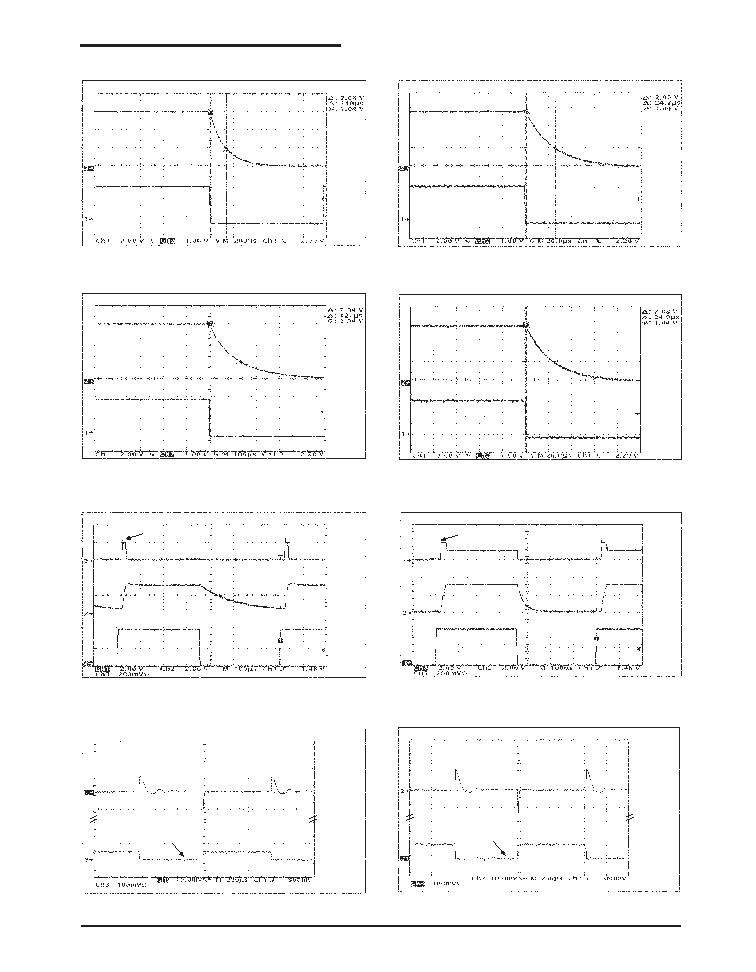
27įC, V
IN
=4V, I
L
= 0.1mA, C
IN
= C
OUT
= 1ĶF unless otherwise specified.
TYPICAL PERFORMANCE CHARACTERISTICS

8
Date: 08/10/05 SP6213, SP6214 Micropower, SC-70, 100mA CMOS LDO Regulator © Copyright 2005 Sipex Corporation
-100
-80
-60
-40
-20
0
Frequency (Hz)
PSRR, DB
10mA
50mA
10
100
1000
10000
100000
1000000
Power Supply Rejection Ratio, V
O
=3V
SP6213-3.0V
OUT
fixed
V
IN
=7V
CTE
C
IN
=C
OUT
=1uF Cer. Cap
T
R
=T
F
=100ns
I
OUT
100uA
V
OUT
20mV
10mV
0mV
-10mV
100mA
0mA
Load Transient Response (V
IN
= 7V)
SP6213-3.0V
OUT
fixed
V
IN
=7V
CTE
C
IN
=C
OUT
=1uF Cer. Cap
T
R
=T
F
=100ns
I
OUT
100uA
V
OUT
20mV
10mV
0mV
-10mV
100mA
0mA
Load Transient Response (V
IN
= 7V)
SP6213-3.0V
OUT
fixed
I
OUT=
100uA
C
OUT
=1uF Cer. Cap
V
IN
V
OUT
5V
4V
5mV
0mV
-5mV
-10mV
Line Transient Response (V
IN
=4V, I
OUT
=100
ĶA)
Line Transient Response
SP6213-3.0V
OUT
fixed
I
OUT=
10mA
C
OUT
=1uF Cer. Cap
V
IN
V
OUT
5V
4V
5mV
0mV
-5mV
-10mV
Line Transient Response (V
IN
=4V, I
OUT
=10mA)
Line Transient Response (V
IN
=7V, I
OUT
=100
ĶA)
Line Transient Response (V
IN
=7V, I
OUT
=10
ĶA)
27įC, V
IN
=4V, I
L
= 0.1mA, C
IN
= C
OUT
= 1ĶF unless otherwise specified.
TYPICAL PERFORMANCE CHARACTERISTICS

9
Date: 08/10/05 SP6213, SP6214 Micropower, SC-70, 100mA CMOS LDO Regulator © Copyright 2005 Sipex Corporation
D
e
E
b
HE
A2
A1
A
Q1
c
L
NOTE:
1. All dimensions are in
inches/(millimeters)
2. Dimensions are inclusive
of plating
3. Dimensions are exclusive
of mold flash & metal burr
4. All specifications comply
to EIAJ SC70
e
SYMBOL
MIN
MAX
e 0.026BSC/(0.65 BSC)
D
0.071/(1.80)
0.067/(2.20)
b
0.006/(0.15)
0.012/(0.30)
E
0.045/(1.15)
0.053/(1.35)
HE
0.071(1.80)
0.094(2.40)
Q1
0.004/(0.10)
0.016/(0.40)
A2
0.031/(0.80)
0.039/(1.00)
A1
0.000/(0.00)
0.004/(0.10)
A
0.031/(0.80)
0.043/(1.10)
c
0.004/(0.10)
0.007/(0.18)
L
0.004/(0.10)
0.012/(0.30)
5 PIN SC-70
PACKAGE: 5 PIN SC-70

10
Date: 08/10/05 SP6213, SP6214 Micropower, SC-70, 100mA CMOS LDO Regulator © Copyright 2005 Sipex Corporation
ANALOG EXCELLENCE
Sipex Corporation reserves the right to make changes to any products described herein. Sipex does not assume any liability arising out of the
application or use of any product or circuit described herein; neither does it convey any license under its patent rights nor the rights of others.
Corporation
Sipex Corporation
Headquarters and
Sales Office
233 South Hillview Drive
Milpitas, CA 95035
TEL: (408) 934-7500
FAX: (408) 935-7600
Part Number
Temperature Range
Package Type
SP6213EC5-1.8 ................................................... -40įC to +125įC .................................................. 5 Pin SC-70
SP6213EC5-1.8/TR ............................................. -40įC to +125įC .................................................. 5 Pin SC-70
SP6213EC5-2.5 ................................................... -40įC to +125įC .................................................. 5 Pin SC-70
SP6213EC5-2.5/TR ............................................. -40įC to +125įC .................................................. 5 Pin SC-70
SP6213EC5-2.7 ................................................... -40įC to +125įC .................................................. 5 Pin SC-70
SP6213EC5-2.7/TR ............................................. -40įC to +125įC .................................................. 5 Pin SC-70
SP6213EC5-2.85 ................................................. -40įC to +125įC .................................................. 5 Pin SC-70
SP6213EC5-2.85/TR ........................................... -40įC to +125įC .................................................. 5 Pin SC-70
SP6213EC5-3.0 ................................................... -40įC to +125įC .................................................. 5 Pin SC-70
SP6213EC5-3.0/TR ............................................. -40įC to +125įC .................................................. 5 Pin SC-70
SP6213EC5-3.3 ................................................... -40įC to +125įC .................................................. 5 Pin SC-70
SP6213EC5-3.3/TR ............................................. -40įC to +125įC .................................................. 5 Pin SC-70
SP6213EC5-5.0 ................................................... -40įC to +125įC .................................................. 5 Pin SC-70
SP6213EC5-5.0/TR ............................................. -40įC to +125įC .................................................. 5 Pin SC-70
SP6214EC5-1.8 ................................................... -40įC to +125įC .................................................. 5 Pin SC-70
SP6214EC5-1.8/TR ............................................. -40įC to +125įC .................................................. 5 Pin SC-70
SP6214EC5-2.5 ................................................... -40įC to +125įC .................................................. 5 Pin SC-70
SP6214EC5-2.5/TR ............................................. -40įC to +125įC .................................................. 5 Pin SC-70
SP6214EC5-2.7 ................................................... -40įC to +125įC .................................................. 5 Pin SC-70
SP6214EC5-2.7 /TR ............................................ -40įC to +125įC .................................................. 5 Pin SC-70
SP6214EC5-2.85/TR ........................................... -40įC to +125įC .................................................. 5 Pin SC-70
SP6214EC5-2.85 ................................................. -40įC to +125įC .................................................. 5 Pin SC-70
SP6214EC5-3.0 ................................................... -40įC to +125įC .................................................. 5 Pin SC-70
SP6214EC5-3.0/TR ............................................. -40įC to +125įC .................................................. 5 Pin SC-70
SP6214EC5-3.3 ................................................... -40įC to +125įC .................................................. 5 Pin SC-70
SP6214EC5-3.3/TR ............................................. -40įC to +125įC .................................................. 5 Pin SC-70
SP6214EC5-5.0 ................................................... -40įC to +125įC .................................................. 5 Pin SC-70
SP6214EC5-5.0/TR ............................................. -40įC to +125įC .................................................. 5 Pin SC-70
ORDERING INFORMATION
Pack quantity is 3000 for SC70-5
Available in lead free packaging. To order add "-L" suffix to part number.
Example: SP6214EC5-3.3/TR = standard; SP6214EC5-L-3.3/TR = lead free
CLICK HERE TO ORDER SAMPLES